
What Is VLSI Design? Design Flow, Applications and Careers
A chip may contain billions of transistors, but its design starts with a much smaller question: what must the hardware do?
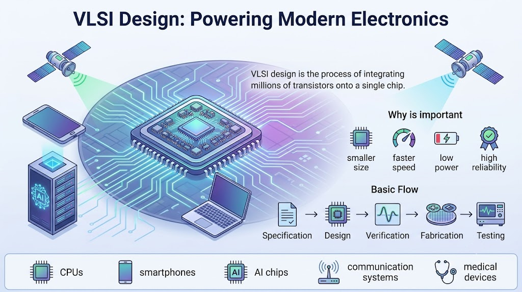
VLSI design is the process of creating integrated circuits with very large numbers of devices on one chip. Digital designs move from requirements and logic descriptions to a physical layout that can be manufactured. Analog and mixed-signal work adds its own circuit and layout methods.
What does VLSI design include?
VLSI stands for very-large-scale integration. The term describes dense integrated circuits rather than a universal transistor-count boundary that every modern design must cross.
A project balances functionality, performance, power, area, cost, and reliability. Improving one can make another harder: faster circuits may consume more power or require more area.
- Digital: processors, controllers, memories, and logic.
- Analog: amplifiers, references, and other continuous-signal circuits.
- Mixed-signal: combinations such as data converters and interface chips.
The digital VLSI design flow
- Specification: define behavior, interfaces, timing, power, and operating conditions.
- Architecture: divide the work into blocks and choose data paths and storage.
- RTL development: describe register transfers and logic in a hardware description language.
- Functional verification: check behavior against requirements using suitable testbenches and other methods.
- Synthesis: map the description into a gate-level implementation.
- Physical implementation: plan the floorplan, power network, placement, clock distribution, and routing.
- Signoff: check timing, physical rules, connectivity, power integrity, and other required conditions.
- Fabrication and test: manufacture, package, and evaluate the silicon.
Real VLSI design is iterative. A physical timing problem can send the team back to architecture, RTL, constraints, or placement.
Verification is more than running a few examples
A test that passes one input sequence doesn’t establish correctness. Verification needs to address reset, corner cases, concurrency, illegal inputs, and the assumptions around each interface.
Simulation, formal methods, coverage analysis, and review can complement one another. Their use depends on the block and project requirements.
Front-end and back-end work compared
| Area | Typical work | Key question |
|---|---|---|
| Architecture and RTL | Behavior, pipelines, interfaces, state machines | Does the hardware implement the intended function? |
| Verification | Tests, assertions, formal checks, coverage | What evidence supports correct behavior? |
| Physical design | Floorplan, placement, clocks, routing | Can the implementation meet physical constraints? |
| Test engineering | Test structures and production test methods | How will manufacturing faults be detected? |
These roles cooperate throughout VLSI design. A clean handoff helps, but treating them as isolated stages often hides problems until late in the project.
A counter as a first design
Consider an 8-bit counter that increments on each clock edge when enable is asserted. Without additional saturation logic, its unsigned value wraps from 255 to 0.
Your specification must state reset behavior, enable timing, and whether wraparound is intended. The RTL is only correct relative to those choices.
A useful testbench checks reset, counting, disabled operation, and wraparound. Timing analysis then asks a different question: can the implemented logic meet its clock requirements?
ASIC vs FPGA: what changes?
An ASIC is manufactured for a particular implementation. An FPGA is a configurable device whose existing resources are programmed to implement logic.
Both can use RTL and verification, but an FPGA bitstream doesn’t fabricate a new chip. Libraries, timing resources, clocking, memories, and physical workflows differ.
FPGA practice can teach valuable VLSI design habits. It doesn’t reproduce every manufacturing and signoff concern of an ASIC.
Skills to build first
- Boolean logic, flip-flops, state machines, and timing.
- A hardware description language such as Verilog or VHDL.
- Testbench writing and waveform debugging.
- Basic CMOS behavior, constraints, and power concepts.
- Scripting, version control, and clear technical documentation.
Career paths include RTL design, verification, physical design, analog design, and test. Requirements vary by role; a working, well-tested project explains your skills better than a list of tool names.
Specify before you code
VLSI design connects a hardware idea to a manufacturable implementation through careful modeling and verification.
Write a short counter specification, implement it, and build tests for reset, enable, and wraparound. Then inspect the synthesized circuit and explain how it matches your intent.

Comments
Comments are currently closed.