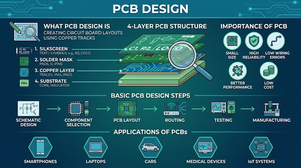
In modern electronics, almost every device—from mobile phones and laptops to medical instruments and industrial machines—relies on a Printed Circuit Board (PCB). PCB design is the process of creating these circuit boards that mechanically support and electrically connect electronic components using conductive pathways.
PCB design is a critical stage in electronics development because it determines the performance, reliability, size, and cost of the final product. A well-designed PCB ensures that electronic components communicate efficiently without noise, overheating, or failure.
This guide explains what PCB design is, its importance, tools used, layers of a PCB, and a step-by-step process to design a PCB in a beginner-friendly way.
What is PCB Design?
PCB design is the process of planning and creating a layout for a printed circuit board that connects electronic components using copper tracks, pads, and vias on a non-conductive board.
A PCB acts as the foundation of almost all electronic devices by replacing bulky wiring systems with compact, reliable circuit connections.
Simple Definition:
PCB design is the process of converting an electronic circuit into a physical board layout that can be manufactured and used in real-world devices.
Importance of PCB Design
PCB design is important because it:
- Reduces circuit size
- Improves reliability
- Reduces wiring errors
- Enhances performance
- Makes mass production possible
- Reduces manufacturing cost
- Improves heat management
Without PCB design, modern compact electronics would not be possible.
Basic Structure of a PCB
A PCB consists of multiple layers that work together to support electrical connections.
1. Substrate Layer
- Base material of the PCB
- Usually made of fiberglass (FR4)
- Provides mechanical strength
2. Copper Layer
- Thin layer of copper on the board
- Forms electrical connections (tracks)
- Can be single or multiple layers
3. Solder Mask
- Protective layer over copper
- Prevents short circuits
- Usually green in color
4. Silkscreen Layer
- Printed labels and symbols
- Helps identify components
- Shows component names and values
Types of PCBs
1. Single-Layer PCB
- One copper layer
- Simple and low-cost
- Used in basic electronics
2. Double-Layer PCB
- Copper on both sides
- More complex circuits
- Used in industrial devices
3. Multi-Layer PCB
- More than two layers
- Used in smartphones and computers
- High performance and compact size
Tools Used in PCB Design
Modern PCB design is done using software tools such as:
- KiCad
- Altium Designer
- Eagle PCB Design Software
- OrCAD
- EasyEDA
These tools help in schematic creation, layout design, simulation, and manufacturing file generation.
Step-by-Step PCB Design Process
PCB design follows a systematic process from idea to manufacturing.
Step 1: Circuit Design (Schematic Creation)
The first step is designing the circuit diagram using schematic software.
In this step:
- Components are selected (resistors, capacitors, ICs)
- Electrical connections are made logically
- Circuit functionality is verified
Output:
A schematic diagram representing the circuit operation.
Step 2: Component Selection
Choosing proper components is very important.
Factors considered:
- Voltage rating
- Current rating
- Power consumption
- Availability
- Size and cost
Correct selection ensures reliable PCB performance.
Step 3: PCB Layout Design
This is the most important step.
In this step:
- Components are placed on the board
- Electrical connections are converted into copper tracks
- Board shape and size are defined
Key considerations:
- Short signal paths
- Proper spacing
- Heat management
- Noise reduction
Step 4: Routing (Track Design)
Routing involves creating copper paths between components.
Types of routing:
- Manual routing
- Auto-routing (software-assisted)
Good routing ensures:
- Minimal interference
- Better performance
- Reduced signal loss
Step 5: Design Rule Check (DRC)
DRC ensures that the PCB design follows manufacturing rules.
It checks:
- Track spacing
- Pad size
- Clearance
- Short circuits
Errors must be corrected before proceeding.
Step 6: Gerber File Generation
Gerber files are the final output files used for manufacturing.
These files include:
- Copper layers
- Solder mask
- Silkscreen
- Drill holes
Manufacturers use these files to produce physical PCBs.
Step 7: PCB Fabrication
In this step, the PCB is physically manufactured.
Process includes:
- Copper etching
- Layer lamination
- Drilling holes
- Applying solder mask
The result is a bare PCB board.
Step 8: Component Assembly (Soldering)
Electronic components are mounted on the PCB.
Methods:
- Through-hole soldering
- Surface Mount Technology (SMT)
This step completes the electronic assembly.
Step 9: Testing and Debugging
After assembly, the PCB is tested for proper operation.
Testing includes:
- Continuity testing
- Voltage testing
- Functional testing
Any faults are corrected during debugging.
Best Practices in PCB Design
To create high-quality PCBs, engineers follow these practices:
- Keep signal paths short
- Use proper grounding techniques
- Separate analog and digital sections
- Avoid sharp 90° traces
- Use proper heat dissipation methods
- Place decoupling capacitors near ICs
These practices improve performance and reliability.
Applications of PCB Design
PCB design is used in almost every electronic industry.
1. Consumer Electronics
- Smartphones
- Televisions
- Laptops
- Home appliances
2. Automotive Industry
- Engine control systems
- Airbags
- Dashboard electronics
- Infotainment systems
3. Industrial Equipment
- Automation systems
- Robotics
- Control panels
- Power systems
4. Medical Devices
- ECG machines
- MRI systems
- Patient monitors
- Diagnostic tools
5. Communication Systems
- Routers
- Modems
- Satellites
- Wireless devices
6. IoT Devices
- Smart home devices
- Wearable devices
- Sensor networks
- Smart agriculture systems
Advantages of PCB Design
- Compact size of circuits
- High reliability
- Reduced wiring errors
- Mass production capability
- Improved performance
- Better durability
Limitations of PCB Design
- Initial design complexity
- High cost for small prototypes
- Difficult modifications after manufacturing
- Requires specialized tools and knowledge
Conclusion
PCB design is a fundamental process in modern electronics that transforms circuit ideas into physical, functional boards. It plays a key role in ensuring the efficiency, reliability, and compactness of electronic devices.
From schematic design to manufacturing and testing, PCB design involves multiple carefully planned steps. With the help of modern software tools like KiCad, Altium Designer, and Eagle, PCB design has become more efficient and accessible.
As electronics continue to evolve, PCB design will remain a critical skill for engineers working in embedded systems, IoT, robotics, and advanced electronic product development.