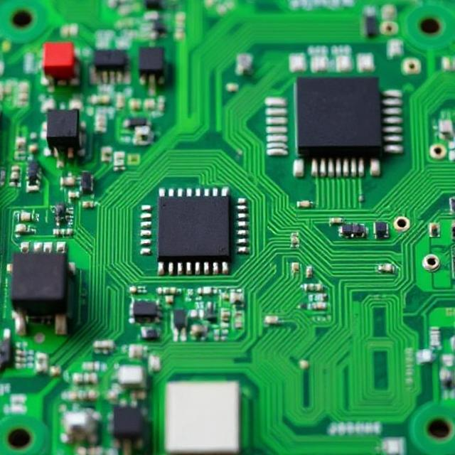
VLSI technology is a complex and highly advanced process that enables the creation of modern electronic devices. Through steps like processing, lithography, interconnects, packaging, and testing, millions of transistors are packed onto a tiny silicon chip, making possible the powerful electronics we use in everyday life.
1. Processing (Chip Fabrication)
Processing refers to the series of steps used to build the tiny components, like transistors, on the silicon wafer (the base material for most chips).
Steps in the Processing Stage:
Wafer Preparation: The process starts with a thin, flat piece of silicon called a wafer. The wafer is typically about 300 mm (about 12 inches) in diameter.
Oxidation: The wafer is heated in an oxygen-rich environment to form a thin layer of silicon dioxide (SiO2) on the surface. This layer acts as insulation.
Doping: Doping is the process of adding small amounts of specific impurities (like boron or phosphorus) to the silicon. This changes the electrical properties of the silicon, making it either a conductor or an insulator, and is essential for making the transistors.
Etching: Etching removes parts of the layers created above to form the desired patterns. Think of it like carving out tiny designs on the surface of the silicon wafer.
Deposition: In this step, thin layers of material, such as metal or poly-silicon, are deposited on the wafer to form the transistors, capacitors, and other components.
Ion Implantation: This is the process of shooting ions into the silicon wafer to “implant” the doping material in precise locations.
Annealing: After ion implantation, the wafer is heated to repair the damage done to the silicon and to activate the doping process.
Lithography
Lithography is the process of transferring a circuit pattern onto the wafer. This is one of the most important steps in creating a VLSI chip.
How Lithography Works:
- A light-sensitive material called photoresist is applied to the wafer.
- A mask is used to create the circuit design. This mask acts like a stencil, allowing only certain parts of the wafer to be exposed to light.
- The wafer is then exposed to ultraviolet (UV) light. The light changes the chemical properties of the photoresist in the areas where it hits.
- The exposed photoresist is developed (like developing a photograph), leaving behind a pattern that matches the mask.
- After this, an etching process is used to remove the exposed material, leaving behind the patterned circuit on the silicon wafer.
Key points about Lithography:
- The resolution (smallest feature size) of the circuit pattern depends on the wavelength of light used and the precision of the process.
- As transistors become smaller, advanced techniques like extreme ultraviolet (EUV) lithography are used.
3. Interconnects (Connecting Transistors)
Once the individual components (like transistors) are created on the silicon wafer, the next task is to connect them together to form functional circuits. This is done using interconnects.
What are Interconnects?
- Interconnects are metal lines (usually made of copper or aluminum) that link the various components (transistors, capacitors, etc.) on the chip.
- These metal lines are deposited over the surface of the wafer and etched into the desired patterns to form paths for electrical signals to travel between components.
Important Considerations:
- The design of interconnects is critical for the performance of the chip. If the paths are too long or poorly designed, it can slow down the speed of the chip.
- As chips get more complex, multiple layers of interconnects are used to connect different parts of the circuit. These layers are separated by insulating materials.
4. Packaging
Once the chips are fabricated and the circuits are built on the wafer, they need to be packaged. Packaging protects the delicate components and allows the chip to be connected to the outside world (like a computer or phone).
Steps in Packaging:
- Wafer Testing: Before packaging, each individual chip (or die) is tested to check if it works properly.
- Dicing: The wafer, which contains many chips, is cut into individual dies. Each die will become a separate chip.
- Mounting: The die is placed on a package(a protective housing), which has tiny metal pins or pads to connect it to other parts of a device.
- Wiring: Small wires are connected from the chip to the package. These wires are usually made of gold or aluminum and are extremely thin.
- Encapsulation: Finally, the die and its connections are protected with a plastic or ceramic material to prevent damage.
Purpose of Packaging:
- Protects the delicate circuitry from damage.
- Provides a way to connect the chip to the motherboard or other parts of an electronic device.
- Helps dissipate heat, as chips generate heat when they work.
5. Testing
Testing is an essential step to ensure that the VLSI chip works correctly and meets the required standards. Without testing, faulty chips would end up in consumer products, leading to failures.
Types of Testing:
Wafer Testing: After the wafer is made but before it’s packaged, each individual chip is tested for basic functionality. This is done using automated equipment to check if the transistors are working correctly.
Functional Testing: After packaging, the chip is tested again to ensure it performs the desired functions, like processing data or controlling devices.
Burn-In Testing: In this test, the chip is operated for an extended period under high stress (e.g., high temperature) to check for defects that may only appear after prolonged use.
Electrical Testing: This ensures that the chip is not only working as expected but also that it meets electrical specifications (voltage, current, etc.).
Test Coverage:
Testing must cover all possible modes of operation of the chip, ensuring there are no defects that would cause it to malfunction under different conditions.
Summary of the VLSI Process
- Processing: The initial step where the silicon wafer is prepared, doped, etched, and deposited to form transistors and components.
- Lithography: A process that transfers the circuit design onto the wafer using light-sensitive materials, allowing the formation of intricate patterns.
- Interconnects: The wiring that connects different components on the chip to form a functional circuit.
- Packaging: The step where the chip is encased in a protective package, and connections are made to allow it to interface with other parts of a device.
- Testing: The final checks to ensure that each chip works properly before it is used in a final product.