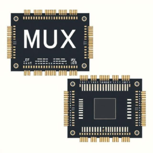
MUX, ROM, and PLA-based designs are fundamental building blocks in VLSI design that enable the creation of complex and efficient digital systems:
Multiplexers (MUX) allow for efficient data routing by selecting one of many inputs based on control signals.
Read-Only Memory (ROM) is used for storing fixed data like firmware or lookup tables, essential for systems that need to reference predefined values.

Programmable Logic Arrays (PLAs) provide a flexible method for implementing complex combinational logic functions, allowing designers to customize logic behavior for specific applications.
Each of these components plays a crucial role in modern VLSI circuits, from microprocessors to memory devices, and is key to designing powerful and efficient digital systems.
Multiplexer (MUX) in VLSI Design
A Multiplexer (MUX) is a digital switch that selects one of many input signals and forwards the chosen input to a single output line. It is often referred to as a “data selector.”
Key Concepts:
- Selection Lines: A multiplexer uses selection lines (or control lines) to choose which input to pass through to the output.
- Inputs and Outputs: A typical multiplexer has 2^ninput lines, where n is the number of selection lines. The output is a single line, which corresponds to one of the inputs.
For example, a 2-to-1 multiplexer has two inputs (A and B), one output (Y), and one selection line (S). The output Y will be A if S = 0 and B if S = 1.
Why MUX is Important in VLSI Design:
- Data Routing: Multiplexers are used for routing data efficiently. They allow multiple data lines to share a single channel, saving space and simplifying design.
- Control Signals: MUX is widely used in digital systems for control purposes. It selects different operations in a microprocessor based on control signals
Read-Only Memory (ROM) in VLSI Design
ROM is a type of non-volatile memory that stores data permanently. It is called “read-only” because, once the data is written during fabrication, it cannot be changed. ROM is widely used in VLSI design for storing fixed information like firmware, look-up tables, or constant data that the system will access repeatedly.
Key Concepts:
- Address Lines: ROM uses address lines to specify which memory location is being accessed.
- Data Lines: These are the output lines that carry the data stored in the ROM location selected by the address lines.
For example, in a 4-bit ROM with 16 locations (i.e., 16 bytes of data), the system will use 4 address lines to select the memory location. The data corresponding to that location will be output.
Types of ROM:
- Mask ROM: Data is written during the manufacturing process, and cannot be modified afterward.
- PROM (Programmable ROM): Data can be programmed after manufacturing, but once written, it cannot be changed.
- EPROM (Erasable Programmable ROM): Data can be erased and reprogrammed using ultraviolet light.
- EEPROM (Electrically Erasable Programmable ROM): Data can be erased and reprogrammed electrically.
Why ROM is Important in VLSI Design:
- Storage of Constants: ROM is used in VLSI designs to store constant values or firmware that doesn’t change over time.
- Lookup Tables: In complex systems like digital signal processors (DSPs) or microcontrollers, ROM can store lookup tables (LUTs) that map input values to output values. This is efficient for performing calculations quickly.
Programmable Logic Array (PLA) in VLSI Design
A Programmable Logic Array (PLA) is a digital device used for implementing combinational logic circuits. PLAs provide flexibility in designing complex logic functions, allowing the user to define custom logic behavior.
The major advantage of PLAs is their programmability, meaning they can be customized to implement specific logic functions based on the designer’s needs.
Why PLA is Important in VLSI Design:
- Flexibility: PLAs are highly flexible because they can be programmed to implement any combinational logic function, which makes them suitable for a wide range of applications.
- Efficient Implementation: In complex circuits, using PLAs can reduce the number of logic gates required and improve overall efficiency.
Design:
- In VLSI, the logic design of a PLA can be customized to include specific AND and OR gates based on the logic function needed.
- A programmable interconnection matrix connects the AND array to the OR array, allowing flexibility in designing custom logic.
PLAs can also be used in place of a set of discrete gates, simplifying the design process and reducing the size of the final circuit.
Tags: 2-to-1 multiplexer, address lines, AND-OR arrays, combinational logic, compact design, constant data storage, control signals, control unit design, custom logic, data lines, data routing, data selector, Digital circuits, digital switch, DSP memory, EEPROM, efficient implementation, Embedded Systems, EPROM, firmware storage, fixed data, hardware programming, input lines, Integrated Circuit, interconnection matrix, logic flexibility, logic gate reduction, logic minimization, logic synthesis, lookup tables, LUTs, mask ROM, memory devices, memory integration, microcontroller memory, microprocessor control, Microprocessors, Multiplexer, MUX, non-volatile memory, output line, PLA, programmable logic, Programmable Logic Array, programmable memory, PROM, read-only memory, ROM, selection lines, Signal Processing, signal selection, VLSI Design


