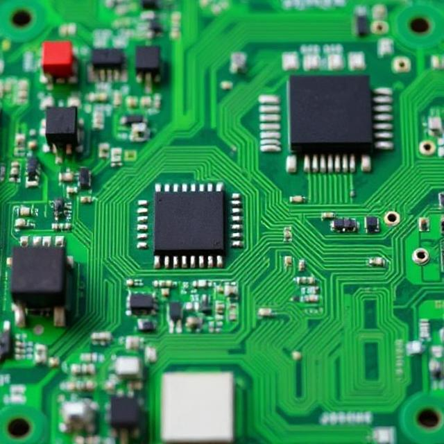
VLSI design is a highly structured and complex process that allows engineers to create powerful chips by integrating millions of tiny components onto a single piece of silicon. The main principles behind VLSI design include abstraction, synthesis, timing, optimization, testability, and power management. By following these principles, engineers can create efficient, reliable, and high-performance chips that power everything from computers to mobile devices.
VLSI (Very-Large-Scale Integration) design refers to the process of creating integrated circuits (ICs) that contain millions of transistors on a single chip. These chips power devices like smartphones, computers, and many other modern technologies. VLSI design is crucial because it allows engineers to pack complex circuits and systems onto a small chip, making electronic devices more powerful and efficient.
Principles of VLSI design in simple terms:
Abstraction and Hierarchy in VLSI Design
Abstraction means simplifying complex systems into easier-to-understand levels. In VLSI design, abstraction helps engineers manage the complexity of designing such intricate chips.
Hierarchy: VLSI design follows a hierarchical approach, which means designing smaller components first and combining them to form a larger system. Think of it like building a house: first, you design the individual rooms (smaller components), then put them together to form the whole house (the chip).
Low-Level Design: At the lowest level, engineers work with transistors and gates.
Mid-Level Design: At the middle level, they combine gates to create more complex circuits like adders or multiplexers.
High-Level Design: At the top level, engineers design the overall functionality of the chip, like the CPU, memory management, etc.
Digital vs. Analog Design
VLSI chips can be designed using digital or analog circuits, or even a combination of both.
Digital Design: This is the most common approach. Digital circuits use binary (0 and 1) signals to perform operations. In digital VLSI design, engineers focus on logic gates, flip-flops, and other components that work with these binary signals. Examples include microprocessors and memory chips.
Analog Design: Analog circuits work with continuous signals, like sound or temperature. VLSI design for analog systems might be used in applications like audio amplifiers or radio frequency (RF) chips.
Mixed-Signal Design: Many VLSI chips have both digital and analog parts, like in audio systems or communication devices, where both types of circuits are needed.
Synthesis and Optimization
Synthesis is the process of converting a high-level design (e.g., a description of how the chip should function) into a physical layout that can be fabricated on silicon. The goal is to transform the abstract design into a real, working circuit.
High-Level Synthesis: At this stage, the engineer focuses on the high-level functionality and begins mapping it into components like logic gates.
Low-Level Synthesis: After that, the design is fine-tuned and optimized, where engineers focus on improving speed, reducing power consumption, and minimizing the size of the chip.
Optimization refers to improving the performance of the chip in areas like:
- Speed: Making sure the chip works as fast as possible.
- Area: Reducing the physical space the chip occupies.
- Power: Minimizing the energy consumption of the chip, which is especially important for mobile devices.
Timing and Clocking
Timing is a key principle in VLSI design because digital circuits are synchronized using a clock signal. The clock determines when specific parts of the chip should perform their tasks.
Clocked Systems: Many digital VLSI circuits are synchronous, meaning they rely on a clock signal to control when each part of the circuit should act.
Timing Constraints: Engineers need to ensure that signals reach the correct components within the time allowed by the clock. If the timing is wrong, the chip might not work correctly, leading to errors.
Clock Gating: This technique is used to reduce power consumption by turning off the clock signal to parts of the chip when they are not in use.
Floorplanning and Placement
Floorplanning is about deciding where different components of the chip will go on the silicon wafer. Since space is limited, this step is crucial to make sure everything fits and works properly.
Placement: Once the floorplan is made, the individual components (like logic gates, memory units, etc.) are placed in the most efficient locations on the chip. This is done to minimize the distance that signals have to travel between components, improving speed and reducing power consumption.
Routing: After placement, the next task is routing, where the interconnects (metal wires) are designed to connect the components. Efficient routing is important to avoid signal delays and congestion.
Design for Testability (DFT)
Design for Testability (DFT) is an approach used to ensure that the chip can be easily tested for defects before it is used in products.
Test Points: Extra components, called test points, are added to the design so that engineers can check if parts of the chip are working correctly.
Scan Chains: These are special circuits added to the design to help test the chip by allowing engineers to test each component in sequence.
Power Consumption and Management
Power management is extremely important in VLSI design, especially for portable devices like smartphones and laptops that rely on batteries.
Dynamic Power: This is the power used when the chip is actively working. It depends on how fast the chip is processing information.
Static Power: This is the power used by the chip when it is idle or not processing. Engineers try to reduce static power by using techniques like power gating (turning off power to parts of the chip when not in use).
Power-Performance Trade-Offs: Designers often need to balance the chip’s power consumption with its performance. For instance, faster processing might use more power, so engineers need to find an optimal balance.
Manufacturing Constraints
Finally, the manufacturing process places physical limits on what can be done in VLSI design.
Process Nodes: The size of the transistors used in VLSI chips is measured in nanometers (nm). Smaller nodes (like 7nm or 5nm) allow more transistors to fit on a chip, making it more powerful, but also harder to manufacture.
Design Rules: These are specific guidelines that engineers must follow to make sure the design can be physically built using available manufacturing technologies. For example, certain features must be spaced far enough apart to avoid defects.
")


 Technology : Explain")