1. What is Schematic Design?
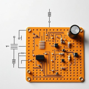
A schematic design is like a blueprint for an electronic circuit. It’s a drawing that shows how all the components in a circuit (like resistors, capacitors, transistors, and wires) are connected together to perform a specific function.
Key Features of a Schematic Design:
- Symbols: Each electronic component, like a resistor or capacitor, has its own symbol in a schematic. These symbols represent the components but aren’t drawn to scale or physically look like the actual parts. Instead, they focus on showing how things are connected.
- Connections (Wires): The lines in a schematic represent electrical connections. They show how the components are connected to each other, like a roadmap.
- Component Values: A schematic design will often include the values of components, such as the resistance of a resistor (e.g., 10 ohms) or the capacity of a capacitor (e.g., 100 microfarads). This helps anyone reading the schematic understand the characteristics of each part.

Example:
Imagine you’re designing a simple circuit with a battery, LED (a light-emitting diode), and a resistor. In the schematic design, you’d see:
- A symbol for the battery (showing the positive and negative sides),
- A symbol for the LED (with the direction of current flow marked),
- A symbol for the resistor (to limit the current to the LED),
- Lines showing how the battery, LED, and resistor are connected.
Schematic design is the first step in designing any electronic system. It helps engineers and designers figure out how the circuit will function without needing to worry about physical layout or the actual components at this stage.
2. What is Circuit Layout?
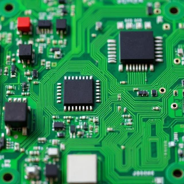
Once the schematic design is complete, the next step is to create the circuit layout. The layout shows how the components are physically placed and connected on a circuit board (usually a Printed Circuit Board or PCB).
Think of circuit layout like a floor plan for your circuit. It details where each component goes on the board and how the electrical connections are routed between them.
Key Features of a Circuit Layout:
- Component Placement: The layout shows where each component (like the battery, LED, or resistor) will be positioned on the physical PCB. The placement is carefully thought out to minimize interference and ensure proper functioning.
- Traces (Electrical Paths): Instead of wires like in a schematic, the layout uses copper traces to show where the electrical connections will go. These traces are like the “roads” that connect the components on the board.
- Via Holes: If a trace needs to go to a different layer of the PCB (because the board has multiple layers), via holes are used. These are small holes drilled through the board to make electrical connections between the layers.
The Layout Process:
- Placing Components: First, the components from the schematic design are placed on the board. The designer has to figure out the best positions for the components, considering factors like size, signal flow, and heat management.
- Routing Traces: After the components are placed, the next step is to route the electrical connections (traces) between them. This is done by drawing copper paths that will carry electrical signals from one component to another.
- Design Rules: The circuit layout needs to follow certain design rules, like making sure the traces are not too thin (so they don’t overheat) or too close together (so they don’t cause short circuits). This ensures the circuit will be reliable.
Example:
In the layout of your LED circuit, the components will be placed on the PCB:
- The battery will go in one corner,
- The LED will be placed in the center where it can easily connect to other parts,
- The resistor will be placed between the battery and the LED. Then, traces will connect them in a way that forms a working circuit.
3. Difference Between Schematic Design and Circuit Layout
| Schematic Design | Circuit Layout |
|---|---|
| It’s a logical diagram showing how components are connected. | It’s a physical layout showing where components are placed on the board. |
| Focuses on functionality of the circuit. | Focuses on the physical arrangement and connections for manufacturing. |
| Symbols represent components. | Actual positions of components on the board, along with traces for connections. |
| No concern for physical dimensions or space. | Concerned with space, size, and routing of electrical paths on the PCB. |
4. Why Are Both Important?
- Schematic design helps you figure out how the circuit should work and allows you to test different ideas without worrying about the physical layout.
- Circuit layout ensures that the design can be turned into a real, physical product that works correctly when assembled.
A well-designed schematic is the blueprint for the circuit, while the layout is the plan for how to actually build the circuit on a physical board.
5. Example to Illustrate Both
Let’s use a simple light control circuit as an example.
- Schematic Design:
- You decide you want a circuit that turns on an LED when you press a button. You start with a schematic.
- You add components: a button, a resistor (to limit current to the LED), and the LED itself.
- You connect them with wires in the schematic, making sure everything is wired logically (so pressing the button completes the circuit and turns on the LED).
- Circuit Layout:
- Now, you move to the layout. You decide the button will go in the top-left corner, the resistor will be placed next to it, and the LED will be in the center of the board.
- You lay out the traces (the copper paths) that will connect the button, resistor, and LED. You also ensure there is enough space between components to avoid overheating and short-circuits.
- Once everything is placed and routed, you have the physical design that can be printed onto a PCB.
Summary:
- Schematic Design: This is the diagram that shows how components in a circuit are connected logically to make it work. It focuses on the functionality of the circuit.
- Circuit Layout: This is the physical design that shows where each component will be placed on the PCB and how the connections (traces) will be routed. It focuses on practical assembly and manufacturing.
Both are essential parts of designing any electronic circuit, as the schematic is where you plan the circuit’s operation, and the layout is how you bring that plan to life on a real circuit board.


