
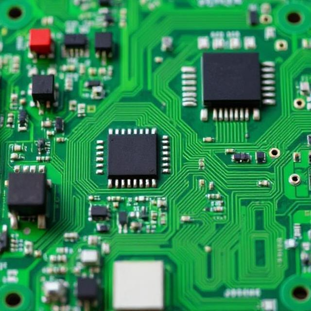
PCB Design and Layout Considerations:
When designing and laying out a Printed Circuit Board (PCB), there are several important factors to ensure the board functions effectively and reliably. These considerations include both electrical and mechanical aspects of the design. Here’s a brief overview of key points to keep in mind:
1. Understanding PCB Layers and Stack-Up
A PCB is made up of different layers, including conductive layers (for traces) and non-conductive layers (for insulation). A single-layer PCB is simple and cost-effective, while multi-layer PCBs provide more complex designs and functionality. Choosing the right number of layers depends on the complexity of the circuit, available space, and desired electrical performance.
Key Considerations:
-
Number of Layers: More layers offer more routing space but increase cost.
-
Stack-Up Design: The arrangement of layers affects impedance control, signal integrity, and overall performance.
2. Trace Width and Spacing
The width of the PCB traces (the copper paths that connect components) plays a significant role in the electrical performance. Too narrow traces can cause overheating or signal integrity issues, while too wide traces may increase cost and take up unnecessary space.
Key Considerations:
-
Trace Width: Determined by the current carrying capacity and the PCB’s thickness.
-
Trace Spacing: Adequate spacing between traces avoids short circuits and ensures reliable operation.
3. Signal Integrity and Grounding
Signal integrity is essential to ensure signals are transmitted without distortion or loss. Grounding techniques and proper layout help prevent noise and interference, which could compromise the signal’s quality.
Key Considerations:
-
Ground Planes: Use a solid ground plane to reduce noise and provide a low-impedance path for signals.
-
Signal Traces: Keep high-speed signal traces as short and direct as possible.
-
Via Usage: Vias (small holes connecting different layers) should be minimized to reduce signal loss and impedance mismatch.
4. Power Distribution and Decoupling
Power integrity is crucial for ensuring stable voltage levels and preventing power-related issues like noise and voltage drops. Decoupling capacitors should be placed near power pins of components to filter out noise and stabilize the supply voltage.
Key Considerations:
-
Power Planes: Create dedicated power planes to ensure stable power distribution.
-
Decoupling Capacitors: Place capacitors close to sensitive components to reduce noise and maintain stable voltage.
5. Thermal Management
Heat dissipation is an often-overlooked aspect of PCB design. If components generate too much heat and are not properly managed, it can lead to component failure or performance degradation. Proper heat sinks or thermal vias can help manage heat buildup.
Key Considerations:
-
Thermal Vias: Use vias to transfer heat from components to other layers.
-
Heat Dissipation: Consider using heat sinks or copper pours to spread heat away from high-power components.
6. Component Placement
Proper component placement is essential for ensuring a clean, functional layout. Components should be placed to minimize trace lengths, avoid interference, and ensure ease of manufacturing.
Key Considerations:
-
Critical Components: Place high-speed or sensitive components in locations that minimize signal path length.
-
Orientation and Spacing: Ensure there’s enough space for thermal expansion and that components are oriented for efficient manufacturing and easy assembly.
7. Manufacturing Constraints
It’s important to design the PCB with manufacturing capabilities in mind. Designers should be aware of the limitations of the PCB fabrication process, including the minimum trace width, via sizes, and board thickness.
Key Considerations:
-
Fabrication Guidelines: Follow the manufacturer’s design rules, such as the minimum trace width, hole sizes, and component spacing.
-
DFM (Design for Manufacturing): Ensure the design is easily manufacturable to avoid extra costs or issues during production.
8. Design for Testability (DFT)
Designing the PCB for easy testing during production is crucial for quality control and maintenance. Test pads, accessible test points, and clear component labeling can save time during troubleshooting.
Key Considerations:
-
Test Points: Provide easily accessible test points for checking voltages and signals.
-
Clear Labeling: Label components clearly to aid in troubleshooting.
9. EMI/EMC Considerations
Electromagnetic interference (EMI) and electromagnetic compatibility (EMC) are important for ensuring the PCB complies with industry standards and doesn’t interfere with other devices. Shielding, grounding, and careful layout can help minimize EMI.
Key Considerations:
-
Shielding: Use copper pours or external enclosures to block unwanted interference.
-
Layout: Avoid running high-speed or noisy signals parallel to sensitive traces.
10. Design Rule Check (DRC)
A Design Rule Check (DRC) is essential to verify that the PCB design meets all the necessary electrical and mechanical specifications before it is sent for manufacturing. It ensures that there are no errors such as trace collisions, incorrect component footprints, or improper clearances.
Key Considerations:
-
Automated Checks: Use DRC tools in PCB design software to identify potential issues early.
-
Final Review: Perform a manual check to catch any mistakes that automated tools may miss.
Conclusion
The design and layout of a PCB involve balancing multiple factors such as signal integrity, power distribution, thermal management, and manufacturing constraints. By considering these aspects early in the design process, you can ensure that your PCB is efficient, reliable, and meets all the functional requirements. Careful planning and following best practices in PCB design can lead to high-performance, cost-effective products that are easy to manufacture and maintain.