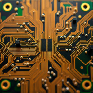
A PCB (Printed Circuit Board) is like the “heart” of most electronic devices. It’s the board that holds and connects all the tiny parts (components like chips, resistors, and capacitors) to make the device work.
PCB Design
Designing a PCB is the process of creating the layout where all the components will go and how they’ll be connected. Here’s how it works:
- Schematic Design: First, engineers draw a basic plan or “schematic” of the circuit, showing how all the components are connected.
- Layout Design: Then, using special software, the engineer arranges the components on the PCB. The goal is to make sure everything fits and is placed in a way that the signals (electrical connections) travel the best way.
- Routing: After placing the parts, the next step is to connect them using electrical “traces” (like roads on a map). This is done using software, which makes sure all connections are correct.
- Final Check: Before moving on, the design is double-checked to avoid mistakes that could cause the board to not work properly.
PCB Fabrication
Once the design is ready, the fabrication process makes the actual physical board. Here’s how it’s done:
- Layer Creation: Most PCBs are made of multiple layers. The first step is to create these layers, usually using copper sheets on a non-conductive material like fiberglass.
- Printing the Design: The design is transferred to the copper sheets using a process like photolithography. This leaves traces on the board where the electrical connections will go.
- Drilling Holes: Holes are drilled in the board to place the components (like chips and connectors).
- Etching: The excess copper is removed, leaving only the needed traces. This is done through a chemical process.
- Soldering Pads: Special pads are created where components will be attached, and the board is ready for the parts to be placed.
- Final Steps: The board goes through tests to make sure everything works before it’s sent to be assembled with the components.
 Design : Explain")