Clock Management in VLSI Design: Explained Simply
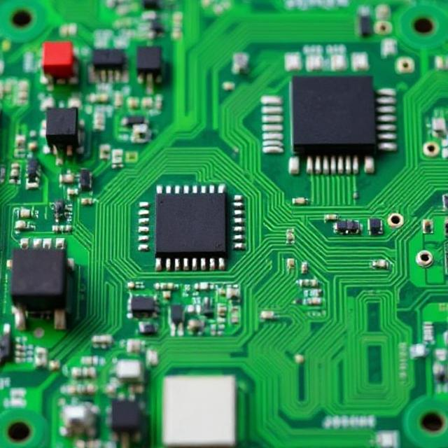
VLSI (Very-Large-Scale Integration) design is the process of creating integrated circuits (ICs) that contain thousands, millions, or even billions of transistors on a single chip. In VLSI design, clock management is a crucial aspect to ensure that the digital circuits work together in a synchronized and efficient manner.
Let’s break down clock management in VLSI design and why it is important, in an easy-to-understand way.

What is a Clock in Digital Circuits?
A clock in digital circuits is like a “heartbeat” that tells all the components (like flip-flops, registers, and logic gates) when to perform their operations. It’s a repeating pulse that synchronizes all parts of the circuit, ensuring that everything happens in a coordinated way.
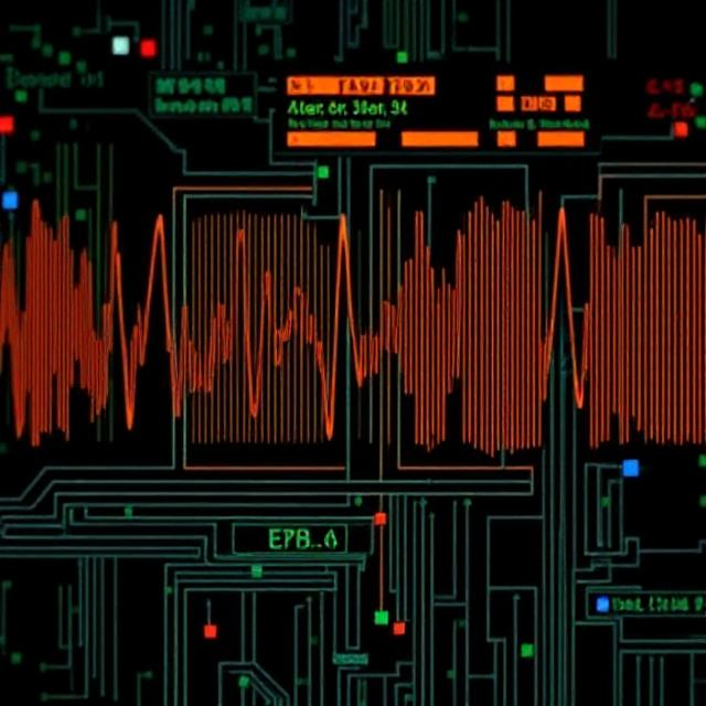
- Clock Signal: A clock signal is a square wave (a pulse that alternates between high and low voltage) that controls the timing of operations.
- Frequency: The clock signal’s frequency (how fast it oscillates) determines how quickly the circuit can process data. The higher the frequency, the faster the circuit operates.
In VLSI designs, clock management involves controlling the timing and distribution of these clock signals throughout the chip.
Why is Clock Management Important?
In modern VLSI systems, the design might have many components working together. Proper clock management ensures that:
- Synchronization: All parts of the chip (like different modules or subsystems) work together at the right time.
- Power Efficiency: Managing the clock properly can reduce power consumption, as circuits only need to work when necessary.
- Speed and Reliability: The clock keeps things running at the right speed, ensuring the system is fast and reliable.
Without good clock management, the components of the circuit could operate out of sync, leading to errors and malfunction.
Key Aspects of Clock Management
- Clock Generation:
- The clock needs to be generated from a stable source (like a crystal oscillator).
- The clock generation circuit creates the clock signal that controls the rest of the system.
- Clock Distribution:
- In a large chip, the clock signal has to travel across many different areas of the chip to reach various components.
- It’s important to distribute the clock signal in such a way that every part of the chip gets the clock at the right time.
- Clock Trees: A clock tree is used to route the clock signal to different parts of the chip. A balanced clock tree ensures the signal reaches all components at the same time with minimal delay.
- Clock Gating:
- Sometimes, you don’t need the clock to run all the time in every part of the chip.
- Clock gating is a technique used to turn off the clock for parts of the circuit when they’re not in use. This saves power by preventing unnecessary switching of transistors.
- This is especially useful in low-power designs like mobile devices.
- Clock Domain Crossing:
- In a large system, different parts of the chip might be running at different clock frequencies (for example, one part might run faster, and another might run slower).
- Clock domain crossing refers to the safe transfer of data between these different clock domains. Special techniques are used to ensure that data doesn’t get corrupted when it moves between components operating at different speeds.
- Clock Skew and Jitter:
- Clock skew is the difference in arrival times of the clock signal at different components. If the clock arrives too late or too early at a part of the chip, it can cause errors.
- Clock jitter refers to small variations in the timing of the clock signal. Too much jitter can cause data to be misread or lost.
- Clock management aims to minimize both skew and jitter to ensure reliable performance.
Techniques Used in Clock Management
- Phase-Locked Loop (PLL):
- A PLL is a circuit used to generate a clock signal that is synchronized to a reference clock (usually from a crystal oscillator).
- It can also be used to adjust the frequency of the clock (e.g., multiplying or dividing the clock frequency), allowing the system to work at different speeds while staying in sync.
- PLLs are essential in VLSI design because they help create stable and accurate clock signals.
- Delay-Locked Loop (DLL):
- A DLL is similar to a PLL, but it is used to align the phases of clock signals rather than adjusting their frequency.
- DLLs are useful for ensuring that the timing of the clock signal is precise and matches the requirements of the system.
- Clock Buffers:
- Clock buffers are circuits used to strengthen or amplify the clock signal before it is sent to different parts of the chip.
- This ensures that the clock signal can travel over long distances without losing its strength and timing integrity.
Challenges in Clock Management
- Power Consumption:
- Managing the clock efficiently is crucial for minimizing power usage, especially in mobile and battery-powered devices.
- Techniques like clock gating (turning off parts of the clock) help reduce unnecessary power consumption.
- Clock Routing:
- The design of the clock distribution network is challenging, especially in large systems. The clock signal must reach all parts of the chip without introducing too much delay or skew.
- Timing Constraints:
- VLSI designs have strict timing requirements. The clock must be synchronized in such a way that data can be reliably read or written at the correct times. Ensuring that everything works within the timing limits is a significant challenge in clock management.
- Clock Noise and Interference:
- The clock signal can interfere with other signals on the chip, especially at high frequencies. Engineers must carefully design the clock system to minimize noise and ensure clean signal transmission.
Summary
Clock management in VLSI design is all about generating, distributing, and controlling the timing of the clock signals throughout the chip. It ensures that the chip’s components work together in a synchronized and efficient manner, saving power and improving performance.
Key tasks in clock management include:
- Clock generation (creating the clock signal).
- Clock distribution (sending the clock to different parts of the chip).
- Clock gating (turning off the clock to save power).
- Managing clock domain crossings (when different parts of the chip run at different clock speeds).
- Minimizing clock skew and jitter (to avoid errors).
Clock management is crucial for creating reliable, efficient, and high-performance VLSI designs, especially in complex systems like smartphones, computers, and other electronic devices.
")