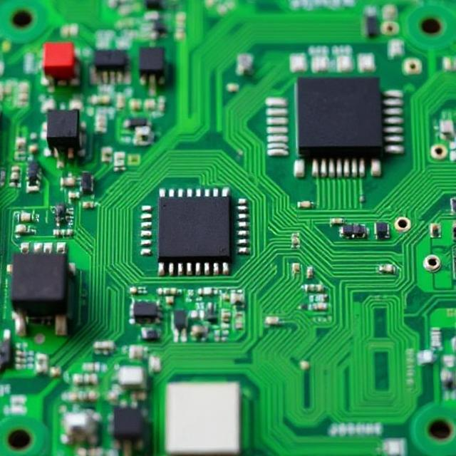
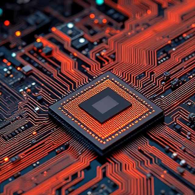
ASIC stands for Application-Specific Integrated Circuit. It is a custom-designed chip made to perform a specific task or function. Unlike general-purpose chips like microprocessors (which can do many tasks), ASICs are optimized for one particular application – which makes them faster, smaller, and more efficient.
Why Use ASICs?
-
High performance for a specific job
-
Low power consumption
-
Small physical size
-
Cost-effective for large production
ASIC Design Flow – Step by Step
Designing an ASIC involves many steps. Here’s a simplified version of the ASIC design flow:
1. Specification
-
Define what the ASIC should do.
-
Includes functional, timing, area, and power requirements.
2. RTL Design (Register Transfer Level)
-
Write the design using a hardware description language (HDL) like Verilog or VHDL.
-
Describes how data moves between registers and logic units.
3. Functional Simulation
-
Simulate the RTL design to check if it works as expected.
-
Detect and fix errors early.
4. Synthesis
-
Convert RTL code into a gate-level netlist (basic logic gates).
-
Optimized for area, speed, and power.
5. Design for Test (DFT)
-
Add features to make testing easier after manufacturing.
-
Includes scan chains, built-in self-test (BIST), etc.
6. Floorplanning
-
Plan the layout of the chip – where major blocks will go.
-
Helps in efficient routing and size planning.
7. Placement and Routing
-
Placement: Place logic gates on the silicon.
-
Routing: Connect them with metal wires.
8. Timing Analysis
-
Make sure the chip meets timing requirements (e.g., clock speed).
-
Check for delays that could cause errors.
9. Physical Verification
-
Check for errors like short circuits, opens, or violations in spacing rules.
-
Use tools like DRC (Design Rule Check) and LVS (Layout vs Schematic).
10. Tape-out
-
Final design is sent to the fabrication facility.
-
This is the step where actual chip manufacturing begins.
11. Fabrication and Packaging
-
The chip is built on silicon wafers.
-
Then it is cut, packaged, and tested.
12. Testing and Validation
-
Test the real chip to make sure it works correctly.
-
Test for functionality, power, speed, and defects.
Types of ASICs
-
Full-Custom ASIC – Everything is designed from scratch. High cost but best performance.
-
Semi-Custom ASIC – Uses pre-designed parts (like standard cells). Faster and cheaper.
-
Gate Array (Structured ASIC) – Pre-designed layout with only part of the chip customized.
Applications of ASICs
ASICs are used in many modern technologies:
| Industry | Applications |
|---|---|
| Consumer Electronics | Mobile phones, smart TVs, tablets |
| Automotive | Airbags, engine control, infotainment |
| Medical | Pacemakers, hearing aids, imaging devices |
| Telecommunications | Routers, network switches, base stations |
| Industrial | Robotics, automation systems |
| Crypto & AI | Bitcoin miners, AI accelerators |
Advantages of ASICs
-
High performance
-
Lower power usage
-
Custom-tailored for a job
-
Smaller size and weight
Disadvantages
-
High initial cost
-
Long development time
-
Not flexible (can’t be reprogrammed)
Summary :
-
An ASIC is a custom chip made to do one specific job really well.
-
The design process starts with writing code, testing it, converting it to logic gates, placing it on a chip, and finally manufacturing it.
-
ASICs are used in everything from smartphones to cars to medical devices.


 Design ?")