Advanced Lithography and Fabrication Technologies – A Brief Summary
1. Introduction
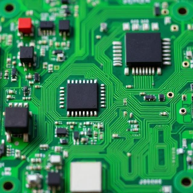
Lithography and fabrication technologies are the backbone of making microchips, sensors, and other tiny devices found in smartphones, computers, and modern electronics. These technologies are used to transfer patterns onto a substrate (usually a silicon wafer), which are then processed to create integrated circuits (ICs) and microelectromechanical systems (MEMS).

As devices become smaller and more powerful, advanced lithography and fabrication methods are needed to create features at the nanometer scale with high accuracy and efficiency.
2. What is Lithography?
Lithography is a process used to transfer patterns (like circuit designs) onto a substrate using light or other radiation.
Basic Steps in Lithography:
-
Coating: Apply a light-sensitive material called photoresist on the wafer.
-
Exposure: Shine light (or another source like electrons or ions) through a mask onto the photoresist.
-
Development: The exposed (or unexposed) areas of the resist are removed to create the desired pattern.
-
Etching: The pattern is transferred into the material below.
-
Stripping: Remaining resist is removed.
3. Types of Lithography Technologies
1. Photolithography (Most Common)
-
Uses ultraviolet (UV) light to pattern the wafer.
-
Resolution is limited by the wavelength of light.
-
Most advanced systems use Extreme Ultraviolet (EUV) light (13.5 nm wavelength) for nanometer-scale features.
2. Electron Beam Lithography (EBL)
-
Uses a focused beam of electrons.
-
Offers very high resolution, useful for research and mask making.
-
Very slow for mass production.
3. Nanoimprint Lithography (NIL)
-
A mold with a nanoscale pattern is physically pressed into a resist layer.
-
Offers high resolution and low cost.
-
Still being developed for high-volume use.
4. X-ray and Ion Beam Lithography
-
Uses X-rays or ion beams instead of light.
-
Can achieve high resolution.
-
Expensive and complex, used mostly in research.
4. Fabrication Technologies
After lithography creates the pattern, various fabrication steps are used to build up layers of materials or remove material.
Key Fabrication Steps:
-
Etching: Removes material selectively (can be dry or wet etching).
-
Deposition: Adds material, such as:
-
Chemical Vapor Deposition (CVD)
-
Physical Vapor Deposition (PVD)
-
Atomic Layer Deposition (ALD)
-
-
Doping: Adds impurities to semiconductors to change electrical properties (done via ion implantation).
-
Chemical Mechanical Polishing (CMP): Flattens the surface for better layering.
These steps are repeated many times to build complex microchips with billions of transistors.
5. Challenges in Advanced Lithography
-
Smaller Features: As chip components shrink below 10 nm, traditional methods face resolution limits.
-
Mask Complexity: Masks become very expensive and hard to make.
-
Alignment Accuracy: Extremely precise positioning is required.
-
Cost: Equipment like EUV lithography machines cost over $100 million each.
6. Recent Developments and Trends
-
EUV Lithography: Replacing older deep-UV methods in advanced chip making (e.g., 5 nm and below nodes).
-
Directed Self-Assembly (DSA): Uses materials that naturally form patterns at the nanoscale.
-
Multi-patterning: Uses several exposures and masks to achieve finer features.
-
3D Integration: Instead of only shrinking features, chips are now stacked vertically (e.g., 3D NAND memory).
7. Applications of Advanced Lithography and Fabrication
-
Semiconductors: CPUs, GPUs, memory chips.
-
MEMS Devices: Sensors in smartphones, medical devices.
-
Photonic Devices: Light-based circuits for high-speed data.
-
Quantum Devices: Requires extremely precise fabrication.
8. Conclusion
Advanced lithography and fabrication technologies are essential for producing the powerful and compact devices we use every day. With the continuous demand for smaller, faster, and more efficient electronics, new methods like EUV, nanoimprint, and 3D integration are pushing the limits of what’s possible.
These technologies play a key role in shaping the future of computing, communication, healthcare, and more, making them critical to modern science and industry.
 Sensors in Automotive Systems")
")

 Technology : Explain")