

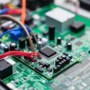
What is PCB Assembly?
PCB assembly is the process of placing and connecting electronic components onto a Printed Circuit Board (PCB) to create a functional electronic device. It involves several steps to make sure all the components are securely attached and properly connected.
Steps in the PCB Assembly Process:
- Solder Paste Printing
The first step is to apply solder paste to the PCB. Solder paste is a mix of tiny metal particles and flux. It’s placed on the spots where the components will go. This is done with a stencil, which ensures the paste is applied in the correct areas. - Component Placement
After the paste is applied, the next step is placing the components onto the PCB. These components can be small parts like resistors, capacitors, and microchips. A machine called a pick-and-place machine picks up each component and places it on the right spot on the PCB. - Soldering (Reflow Soldering)
After the components are placed, the PCB needs to be heated to melt the solder paste. This process is called reflow soldering. The PCB is passed through a heated oven, where the paste melts, creating strong connections between the components and the board. - Inspection (Automated Optical Inspection – AOI)
Once the soldering is done, the board is checked for defects. This is usually done using a machine that takes pictures and checks if everything is correctly placed, soldered, and free of any issues like missing components or poor solder joints. - Through-Hole Component Assembly (if applicable)
Some components, like large connectors or certain types of chips, are “through-hole” components. These components are inserted into holes in the PCB and then soldered on the other side. This can be done manually or with automated machines. - Wave Soldering (if necessary)
For through-hole components, wave soldering is often used. The PCB passes over a wave of molten solder, which flows up into the holes and makes the connections. This process can happen right after reflow soldering. - Cleaning
After all soldering steps are done, the PCB is cleaned to remove any flux residue or other contaminants that could interfere with the circuit’s performance. This is done using chemicals or ultrasonic cleaning. - Final Inspection and Testing
Once the PCB assembly is complete, it undergoes a final inspection. This could involve electrical testing to make sure all components are working correctly, and sometimes functional tests to verify that the whole device works as expected. - Packaging and Shipment
After testing and inspection, the completed PCBs are packaged and ready to be shipped to customers or used in final product assembly.
Summary:
The process can vary slightly depending on whether you’re doing hand assembly, small batches, or high-volume production, but these are the basic steps in PCB assembly
Tags: assembly line, automated optical inspection (AOI), automated soldering, board reliability., circuit connections, cleaning process, component placement, defect detection, electrical testing., Electronic Components, electronics production, flux removal, Functional testing, high-volume assembly, inspection, manual soldering, molten solder, packaging, PCB, PCB assembly, PCB fabrication, PCB manufacturing, pick-and-place machine, Printed Circuit Board, Quality Control, reflow oven, reflow soldering, shipment, solder paste, stencil printing, surface-mount technology (SMT), through-hole components, ultrasonic cleaning, wave soldering