Circuit board etching is the process used to create the electrical pathways (called traces) on a printed circuit board (PCB). These pathways allow electricity to flow between the different components on the board, like resistors, capacitors, and chips, so that your device works. Think of it as the “roads” that connect all the parts of the circuit.
Here’s how it works in simple steps:
1. What is Etching?
Etching is the process of removing unwanted parts of the material on the circuit board to leave behind only the areas that will carry electrical signals. In most cases, the material being removed is copper, which is used to make the pathways or “traces” on the board.
2. How Does the Etching Process Work?
The basic steps in the etching process are:
Step 1: Designing the Circuit
First, the design of the circuit (how the components are connected) is made using special software. The design shows where the copper traces should be on the PCB.
Step 2: Applying a Protective Layer
The circuit board is coated with a layer of photosensitive material, usually a thin film called “photoresist.” This material is sensitive to light and can be hardened by exposure to ultraviolet (UV) light.
Step 3: Exposing the Board to UV Light
The design of the circuit is printed onto a transparent film, and the circuit board is placed under UV light. The parts of the photoresist layer that are exposed to the UV light will harden, while the parts that aren’t exposed will stay soft.
Step 4: Developing the Board
After exposure, the board is washed in a chemical solution that removes the unexposed (soft) parts of the photoresist, leaving only the hardened parts behind. This hardened layer protects the copper beneath it, where the traces will remain.
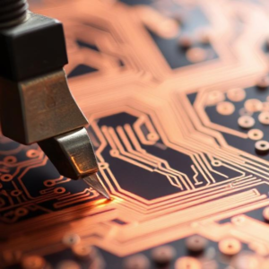
Step 5: Etching the Copper
Now, the board is submerged in a chemical etching solution (usually a mix of acid or salt). The solution eats away at the exposed copper areas, but it leaves the copper protected by the hardened photoresist intact. After the etching process, only the desired copper traces remain on the board.
Step 6: Removing the Photoresist
Finally, the remaining photoresist layer is removed, leaving behind just the copper traces, which will carry the electrical signals between the components on the board.
3. Why is Etching Important?
Etching is a key step in making PCBs because it defines the actual pathways that the electrical signals will follow. Without etching, there wouldn’t be any way for the components to connect and communicate with each other.
4. Different Etching Methods
- Wet Etching: This is the method we just described, where the board is submerged in a chemical solution to remove the unwanted copper.
- Dry Etching: Instead of using a chemical solution, dry etching uses gases to etch away the copper. It’s more precise and is often used for advanced circuit boards, like those in smartphones or computers.
5. Etching Safety
Because etching involves chemicals that can be harmful, it’s important to do it in a controlled environment with the proper safety gear, like gloves and goggles, and make sure the area is well-ventilated.
Summary:
Circuit board etching is the process of creating the copper pathways on a PCB by removing unwanted copper using a chemical solution. It’s like carving out roads on the board that allow electricity to travel between the components. This process involves designing the circuit, protecting areas you want to keep, and using chemicals to etch away the excess copper, leaving only the necessary traces behind. It’s a crucial step in creating the electronics that power your devices!
 Design : Explain")